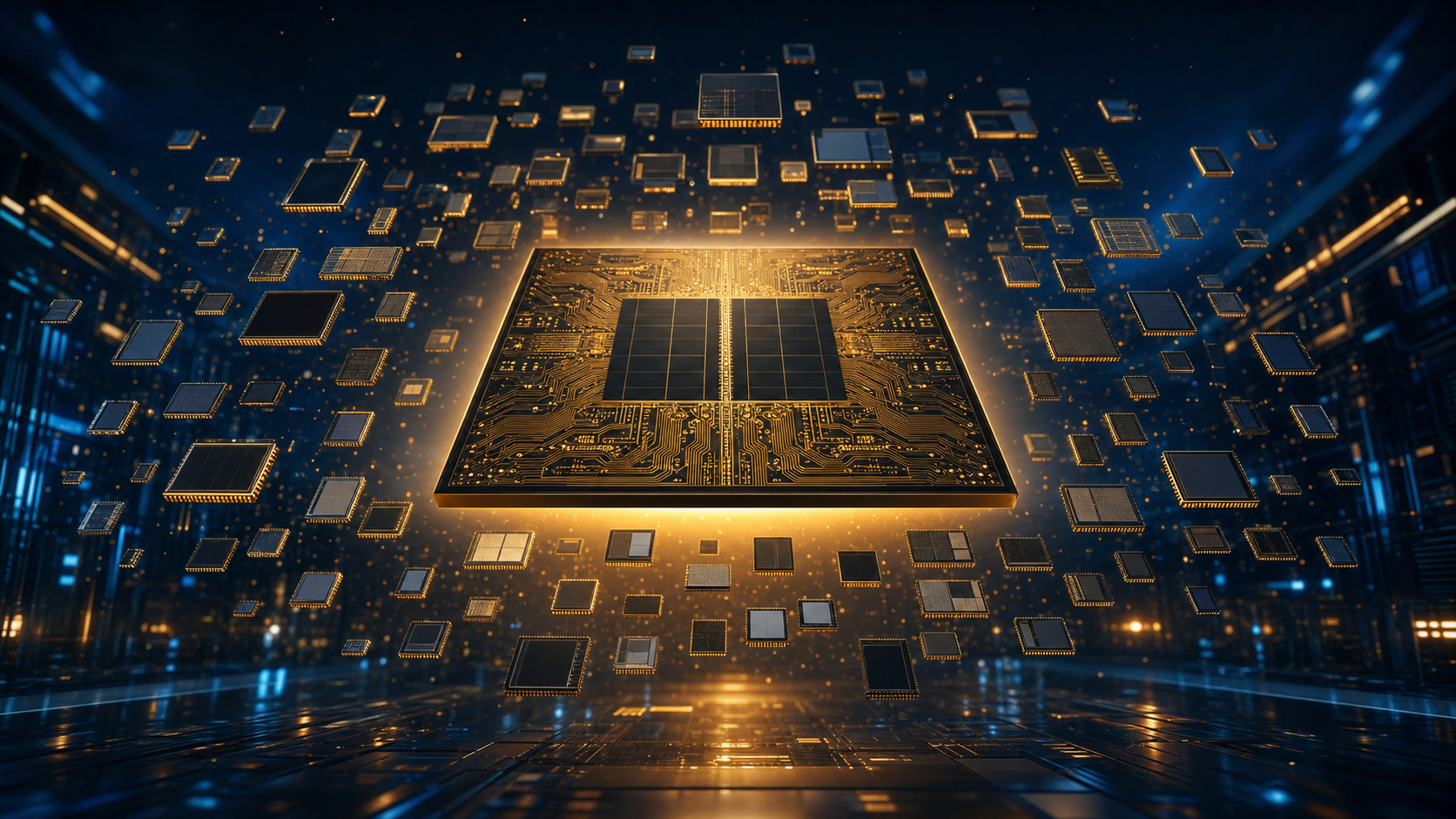
As NVIDIA’s AI chips grow larger with every generation, the entire semiconductor industry has hit a traffic jam in a stage you’ve probably never heard of — not the process node, not the memory, but the packaging.
Over the past two years, the bottleneck in advanced packaging capacity has very tangibly throttled the supply of AI compute. TSMC’s CoWoS slots are nearly impossible to come by, and the inherent geometric limits of round silicon wafers keep the packaging cost of large AI chips stubbornly high. As a result, a technology once dismissed as a “lifeline for panel makers” has suddenly been pushed center stage.
It is called FOPLP (Fan-Out Panel-Level Packaging). In the plainest terms, it swaps the packaging “plate” from a round silicon wafer to a large, square glass panel. It sounds like a mere change of shape, but this shift is igniting a new war among foundries, OSAT packaging giants, and panel makers.
Why Advanced Packaging Became the Chokepoint of AI Compute
To understand why FOPLP matters, you first have to grasp a counterintuitive fact: in the AI era, what determines how powerful a chip is no longer comes down to how small the transistors are, but how many chips — and how much surface area — you can stitch together.

As computing demand approaches its physical limits, the industry’s answer is “heterogeneous integration” — packaging multiple chips, such as compute dies and HBM high-bandwidth memory, onto the same substrate to work in concert. TSMC’s CoWoS is the star technology under this logic, enabling HBM4 to integrate tightly with the GPU and deliver the staggering bandwidth the Rubin generation demands (financialcontent.com).
The problem lies in the carrier. CoWoS uses a round 12-inch silicon wafer as its plate, but AI chips are getting larger and more rectangular. Fitting square chips onto a round wafer causes severe waste at the corners, and the silicon substrate itself is expensive — pushing per-package costs to jaw-dropping levels. Powertech Technology has disclosed one case: a major customer using a 2nm high-end SoC paired with 12 HBM stacks reached a total packaging cost of US$25,000, a rarely seen ultra-high-value packaging design (IEK).
In other words, packaging has been upgraded from the “final finishing step of the process” into the chokepoint that determines the cost and supply of AI chips. Whoever solves area utilization and cost holds the key to the next round of AI compute expansion.
What FOPLP Is: The Leap from Wafer-Level to Panel-Level
Traditional fan-out packaging is called FOWLP (wafer-level) and uses a round wafer. FOPLP’s core breakthrough is a single sentence: swap the round plate for a square one.
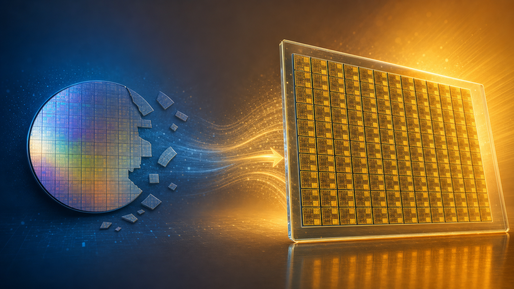
The power of this change is clear from the numbers. Take panel maker Innolux: its FOPLP line uses a 700×700mm square glass substrate, roughly equivalent in area to 6.9 twelve-inch wafers, with a square-substrate area utilization as high as 95% — far surpassing the effective area lost to corner truncation on a round wafer (Economic Daily News). Research firms also note that, against the backdrop of AI chips’ rapidly expanding packaging-area needs and persistently tight CoWoS capacity, panel-level packaging is viewed as an important medium-to-long-term complement (Wistock).
The most pivotal technical consensus of 2026 is the rise of glass substrates. As chip sizes grow, traditional organic materials (such as ABF carriers) are prone to “warpage” and thermal instability, which can ruin a multi-thousand-dollar AI chip during bonding. The glass panels TSMC is verifying with partners like Corning offer roughly 10x higher interconnect density and superior structural integrity (financialcontent.com).
But make no mistake — this road is not easy. Panel-process line widths are currently around 1 micron, while semiconductors are measured in nanometers (1 micron = 1,000 nanometers), an enormous precision gap. Solving the copper-plating and flatness of through-glass vias (TGV) requires high-end lithography machines starting at over NT$300 million each, and the chemical-mechanical polishing (CMP) and lithography of large panels bring entirely new yield challenges (TechNews). Yield is the true decider of this game.
The Battleground: A Three-Way War Among Foundries, OSATs, and Panel Makers
Precisely because FOPLP’s potential is huge and its barriers high, it has become a new battleground where three forces collide.

The first tier consists of TSMC and the two OSAT champions, who hold the advantage in customers and process integration. TSMC chairman C.C. Wei has made clear the company is investing in panel-level packaging and expects the technology to mature by 2027, with its InFO-PLP positioned on the medium-to-long-term roadmap (Kyopt). OSAT leader ASE has been developing fan-out panel-level packaging for over a decade, spending US$200 million on equipment last year, and has advanced its spec from 300×300mm to 600×600mm — if yields hold, 600×600 could become the mainstream spec. Powertech built its line as far back as 2016, has begun low-volume shipments, and has a major customer’s 2nm high-end product in qualification (IEK).
The second tier consists of panel makers hoping to turn their fortunes around. Innolux, once branded a “sunset industry,” used FOPLP to break into SpaceX’s low-Earth-orbit satellite chip supply chain, sending its stock soaring more than 128% in two and a half months (TechNews). By converting its legacy Gen 3.5 panel line, Innolux has already won orders from NXP and STMicroelectronics, runs at full capacity, and the market keeps buzzing about a potential collaboration with TSMC at its Longtan facility (CMoney).
Interestingly, not everyone is bullish. AUO — the other of the two panel giants — has a president, Frank Ko, who has bluntly said FOPLP’s “cost-benefit ratio” is unattractive; rather than pour tens of billions into R&D for thin processing margins, the company is betting heavily on silicon photonics (CPO) and has joined the SEMI silicon-photonics consortium led by TSMC and ASE (TechNews). Meanwhile, Samsung Electronics pioneered FOPLP on the Galaxy Watch processor back in 2018 — the world’s first volume production — but stumbled on the path to large-area AI packaging (Kyopt). This three-way war exists precisely because large AI customers, eager to diversify supply-chain risk, are actively cultivating a “second source” beyond TSMC and ASE, giving panel makers and second-tier OSATs a structural opening to chase design wins (Wistock).
Investment and Technical Takeaways: How Retail Investors Should Read This New Battleground
The story is sexy, but viewed through an engineer’s logic, the devil is in the numbers.

The first thing to recalibrate is the gap between “narrative” and “real contribution.” Yole Group estimates that the panel-level packaging market will grow at a CAGR of over 30% between 2022 and 2028, yet projects total 2028 output value at only about US$1.1 billion — a clear sign this is still an early-stage market (TechNews).
The second thing to see clearly is each stock’s revenue contribution. Take the surging Innolux: the market estimates FOPLP will account for only 2% to 3% of its revenue in 2026. Against its annual revenue of over NT$220 billion, the new business’s near-term earnings contribution is actually quite limited, with the company’s main profit and loss still hinging on panel prices and automotive panel sales (TechNews). In other words, the stock’s surge is buying the imagination of a re-rating, not present-day profit.
The third key metric is yield and customer-qualification progress. As of the first half of 2026, FOPLP remains in a transitional phase “moving from R&D toward small-scale production,” not yet in mainstream high-volume commercial manufacturing (Wistock). For investors, rather than chasing every collaboration rumor, it’s better to watch three things: whether customer qualification passes, whether yield data meets targets, and when revenue contribution truly ramps.
Returning to the cognitive level, FOPLP is a classic story of “structurally correct trend, slow real-world execution.” On trend, AI compute demand will indeed keep driving advanced packaging forward — that part is barely in doubt. On execution, who can clear the yield and customer-trust thresholds remains unknown. For ordinary investors, understanding this time lag — that “right direction does not equal making money now” — matters more than chasing a single stock’s limit-up. It is still far too early to declare who the final winner of this new battleground will be.
Disclaimer: This article is a sharing of industry trends and technical observations only. The companies and data cited are drawn from public information and do not constitute any investment advice or buy/sell recommendation. Investing involves risk; readers should evaluate independently and take responsibility for their own investment decisions.
Comments